Interfacing the Raspberry Pi to 5V Logic
Assume you have some nice 5V only chip you want to use with the Raspberry Pi. In my case it is a MAX1226 A/D converter, I got from Maxim as a free sample that is left over from another project. The Pi uses 3V3 I/O levels. What to do? When I tried to research this on the web, I found a lot of wrong information, missing information and dire warnings that miss the point. Hence, I decided to do a write-up on how things really are.Warning: Now for my own dire warning: While the statements made here are likely correct and represent long-standing best practices in the electronics industry, they may be wrong. So everything I say here may be wrong and if you do damage as a consequence of believing me, I am not responsible.
Well, onwards with the analysis. First, you need to know that digital inputs need to have protection or they will die in normal operation. The reason is that switching of neighbouring signal lines can induce voltage spikes way above Vcc and way below GND. The inputs need to be able to survive that.
The standard way is to just put in protection diodes. Unfortunately the Pi seems to only have normal protection diodes to GND, not to 3V3. What I found in some measurements is that the protection against positive overvoltage seem to be some kind of passive Z-Diode-like scheme. I measured about 6.4V Voltage at 100uA input current and 7.5V at 0.5mA on several differtent inputs, regardless of whether the Pi was switched on or off. At 5.5V input voltage, I measured about 2.4uA input current.
This is in line with the typical protection circuit for a 5V-tolerant I/O pin. I cannot confidently state that without a look into the (missing) datasheet that GPIO on the Pi is really 5V-tolerant. It could be untested, or defective by design or manufacturing. What I can say is that on my Pi, connecting an input in input mode directly to 5V would not kill it, the currents flowing are just way too small.
Organization
First I give my recomended interface method. Then I explain why it works. Unfortunately, some of this is guesswork as the Raspberry Phi has one glaring design mistake, namely selection of a chip with a not publicly available datasheet. (Well, I guess there were some good reasons for that, but it sucks nonetheless.)Update 12/2013: Apparently parts of the Pi community are very much concerned that I do not know what I am takling about and that the approach I present here will kill the I/O-pin. See Raspberyy Pi Forum for a discussion. While unlikely, it is possible that the manufacture included defective I/O circuits and protection in the SoC used in the Pi. Now, there is a statement by "Liz", that 4.3V would be fine, see Liz on 5V I/O. For that reason, I have added the missing upper protection diode externally and now this circuit should really be unable to kill the I/O pin as the voltage at the I/O-pin with the diode will in not exceed 4.3V unless you put in much more than 5.5V. The diode does not impact functionality and the I/O pin remains fully bi-directional. BTW, the pull-up and pull-down circuits I give on GPIO Startup are not affected, there the I/O pin is already at or below 4.3V, so no need to add a diode.
I also have to say that I found the level of actual skill and knowledge in that forum rather low, and the level of arrogance rather high, with wrong and partially wrong "information" being pushed aggressively by some wannabe "alpha posters". There seems to be no interest into actual insight either, but rather people are defending imagined "truths" instead, which makes the forum pretty dysfunctional. Hence, I would advise not to trust anything said there without independent verification.
How to interface a GPIO pin to 5V logic
The very brief version is to just use a 1KOhm series resistor, regardless of whether the GPIO pin is used as input, output or both. Set drive strength as you like. You must turn off pull-up and pull-down resistors for this to work correctly: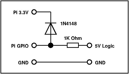
Note: If you are interfacing 3.3V CMOS logic, you can leave the resitor and diode in! That will protect you from killing your Pi if you accidentally conect an I/O pin to 5V.
Note: This does not apply to the two I2C pins that have pull-up resitstors on the board, they need a proper I2C level-shifter. More below.
Effect: This will in effect make the pin 5V-tolerant for digital I/O and will work as long as the 5V circuit interfaced does not have more than 1 LS-TTL load input current. That means it will work for for most CMOS circuits, like the MAX1226 SPI A/D converter. It will also work for basically all TTL-compatible CMOS logic families like 74HCT, 74ACT, 74LVC, etc. The thing to look for in the datasheet is the minimum input H voltage, typically called V_IH. it should be at or below 2.4V for this to work reliable.
For CMOS-level digital signals, where the Pi GPIO pin is used only as input, you can still use this scheme. But driving CMOS-level inputs from a Pi GPIO pin used as output is at the very least unreliable, as these inputs need 3.3V for a solid H, and that is difficult to generate from a 3.3V supply. Here, you need a proper dual-voltage level-shifter, such as the one described for I2C below or you need to add a pull-up resitor of 1 kOhm to 5V. Fortunately, digital circuits requiring CMOS-level input signals are rare today.
Why does this actually work? The input case.
When a Pi GPIO pin is used as input, there are two cases:- The signal going in is L-level. In this case, there is no problem as the GPIO basically has no input current and the 1kOhm resistor has no effect.
- The signal going in is H-level. In this case the diode will limit the Pi input voltage to 4.3V or less (the "Liz-approved value"). The diode a maximum of 1V at 10mA, which would require you to apply 14V or more to reach. Hence the Pi is completely safe at 5V input.
Why does this actually work? The output case.
When a Pi GPIO pin is used as output, there are two cases:-
The signal going out is L level. Typically that means 0.4V
maximum output level and TTL compatible input require
no more than 0.8V input level for a solid L. If the
input is CMOS, it basically has not input current, and
the resistor has no effect. If it is a bipolar input,
1 LS-TTL level will have up to 0.32mA flowing out of the
input, which will raise the signal level to 0.72V, staying
well in spec.
Note that this is why you cannot use the 1kOhm technique with TTL inputs having a higher load. For example, a standard TTL input has up to 1.6mA flowing out of in on a L, which would push the input voltage it sees up to about 2V and right into the forbidden zone. (Yes, bipolar TTL inputs have an output current when an L signal is applied. The explanation why is out of scope of this document.)
- The signal going out is H level. Here I have to speculate. One source incorrectly lists V_IH = 1.4V as the minimum guaranteed output voltage, while it is in fact the minimum required input voltage for a solid H. The correct parameter V_OH under rated load (see output drive strength) is very likely around 2.8V or higher. CMOS inputs take no input current and TTL compatible inputs requre usually 2.0V minimum (in some cases 2.4V) for a solid H, and there is no problem. Note that bipolar TTL inputs have very low input current for H input signals and the same reasoning applies.
Signal propagation delay
In the absence of a datasheet, I would specylate that the overall input capacity of a GPIO pin is below 20pF. That would mean the 1KOhm resistor adds something like 20ns propagation delay. As the software interface is not that fast and time-accurate, this will not matter for GPIO usage. The same holds for the output direction, where 20pF is a reasonable upper value for the input capacity of most circuits. But take care that standard 1.27mm pitch flat ribbon cable has about 50pF/m wire-to-wire, i.e. about 100pF/m when you take into account that most wires have two neighbours.
SPI
The SPI bus is different as it allows higher transfer rates under hardware control. As far as I can determine, the Pi SPI interface has a maximum clock rate of 125MHz. At this rate the 1KOhm resistor will introduce unacceptable delays. But note that even ordinary wiring is a problem at this frequency and that most SPI chips cannot deal with a bus this fast anyways. With the 1kOhm resistor, I recommend not using SPI speeds over 5HMz. In fact, unless you have clean wiring and clean ground, I recommend limiting SPI speed to 1MHz. Most applications will still be fine. If you need more, I recommend using a 3V3 SPI target or a level-shifter like the 74LVC125.I2C
The I2C bus is an open-collector/pull-up-resistor bus. As such, a series resistor is something to avoid and normal level-shifters do not work because they are not bi-directional.If you use the two I2C GPIO pins as normal outputs, you can still use the 1kOhm design, but it fails for input and I2C mode. For that you need a bi-directional level shifter.
The authorative reference is by NPX (used to be Philips), described in this Applicatio Note. (NPX seems to not have it online anymore. Thanks to Adafuit for providing a copy!) The SMD FETs are a bit tricky to handle, but you can roll your own level shifter following this document. You can also get them pre-assembled, e.g. from Sparkfun, just search for "Logic Level Converter". Make sure to connect the higer voltage to "HV" and the lower one to "LV" and use only the "TX" conections, the "RX" ones are not bi-directional.
Also note that these level-shifters are relaticvely slow, and can add 100ns delay or more. For I2C with a maximum clock rate of 400kHz, that is fine. But shifing a fast SPI bust this way is unlikely to work or may not be reliable.